


- I. Technological possibilities of our assembly line:
AUTOMATIC SMT ASSEMBLY
PROTOTYPE ELECTRONICS PRODUCTION
SERIAL ELECTRONICS PRODUCTION
Maximum number of feeders (for 8mm tapes):
180 pcs.
96 pcs.
Maximum dimensions of SMD component package:
33 × 33 mm (acceptable 50 × 50 mm)
100 × 55 mm
Smallest dimensions of SMD component package:
0603, 0402, 0201, 01005
0201, 01005, 009005, 008004
Height of SMD components:
from >0 mm to 10 mm (optionally 15 mm)
from >0 mm to 15 mm
Repeatability of placement:
≤ 50 µm
≤ 25 µm
Linear resolution:
5 µm
1 µm
Rotation resolution:
0.01°
0.01°
Maximum dimensions of PCB:
400 × 300 mm (acceptably: 450 × 350 mm)
510 × 460 mm
PCB thickness:
0.5 - 3.5 mm
0.4 - 4.5 mm
Minimum spacing from PCB edge:
2 mm
2 mm
Clearance under PCB:
40 mm
40 mm
Additional information:
- laser alignment of components;
- laser system for position correction of small components or components with a small lead pitch.
- 2 × fiducial cameras;
- side camera;
- camera for components up to 12 (W) × 12 (L) × 6.5 (H) mm (scan camera);
- MFOV camera for large components up to 100 (W) × 55 (L) × 15 (H) mm in size (large fixed camera).
SCREEN PRINTING
PROTOTYPE ELECTRONICS PRODUCTION
SERIAL ELECTRONICS PRODUCTION
Maximum size of PCB board/panel:
380 mm (L) × 305 mm (W)
450 mm (L) × 390 mm (W)
Clearance under PCB:
10 mm
40 mm
Accuracy of adjustment:
≤ 30 µm
≤ 20 µm
REFLOW SOLDERING (SMT)
Maximum width of PCB board/panel:
0 - 300 mm (W)
Number of zones:
6 (3 × preheating, 2 × soldering, 1 × cooling)
Temperature range:
0 - 500°C
Drive type:
- chain drive (soldering PCB with two assembly layers)
Maximum heating power (total):
- 23 kW (power of all heating zones)
Control:
- microprocessor (PC software - RS485 interface), 16 × temperature sensor
WAVE SOLDERING (THT)
Maximum dimensions of PCB board/panel:
350 mm (L) × 180 mm (W)
Temperature range:
0 - 400°C
Average soldering speed:
ca. 1PCB / 5sec.
Control:
- microprocessor (electronic control temperature)
Possibilities:
- Adapted for lead-free soldering
- II. What do we need to define the electronics production price?
To estimate the cost of electronics assembly, we will need the following technology files:
1️⃣ QUOTE OF PCBs:
- Gerber files
- NCDrill / NCMill files
- information on the PCB design (total thickness, copper thickness, number of layers, soldermask colour, colour of the silk layer, surface finish, etc.).
2️⃣ QUOTE OF ELECTRONIC COMPONENTS AND ASSEMBLY:- BOM list
- Pick&Place file(s) (recommended)
- III. Design of printed circuit boards (PCB) adapted for serial electronics production
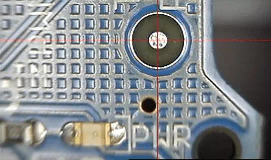
- 1. Reference points (fiducials) and their implementation
It is recommended that a fiducial was formed in the copper layer. Copper may be further secured by a layer of metal (e.g. in the process of gilding or tin plating). Differences between markers on a single PCB should not be larger than 25 µm. The area around the optical marker should be unveiled (directly unveiled laminate). This area may not be covered with solder mask, conductive paths or fragments of electronic components, etc., should not be placed there either.
NOTE! During SMT stencil design, fiducials should be omitted (solder paste may not be placed onto fiducials)! - 2. Shape and size of reference points (fiducials)
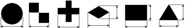
It is recommended that fiducial is oval (although our machines also allows to read other shapes of fiducials - these shapes are shown in the figure below). It is not recommended to use other symmetrical shapes than those shown in the figure below. The size of the marker (diameter) may vary between 1-3 mm. Ideally, if this value is 1-1.5 mm. The diameter of the area around the marker should be 2-3 times larger than the diameter of the fiducial.
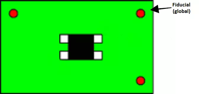
- 3. Number and deployment of reference points (fiducials) - global
Minimum two (recommended three) global fiducials are required for the machine to determine the position of PCB in space. Fiducials should be deployed in close proximity to opposite corners of the printed circuit board (board edges). Remember to shift each marker from the edge of the plate by min. 5 mm. In case the panel (including printed circuit boards) is used, additional fiducials are necessary in the corners.
- 4. Number and deployment of reference points (fiducials) - local
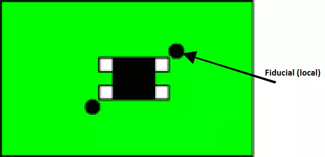
When assembled components have large number of pins and a small grid (i.e. high density of pins, therefore the distance measured between the centers of adjacent pins is less than 0.6 mm), use local fiducials. Two local fiducials diagonally deployed to the casing are necessary for one component.
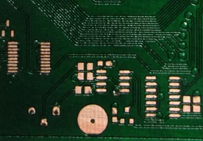
- 5. Electronic components - packages dimensions
The table below shows the standard and most commonly used casings. Our assembly line allows the use of non-standard casings, e.g. electromagnetic shields or M2M circuits.
SMD CHIP PLCC QFP SO TANTALUM OTHERS 2512 PLCC128 QFP208 SOJ28 Tantalum 7343 7814J 2321 PLCC100 QFP196 SOJ24 Tantalum 7243 D Pack 2225 PLCC84 QFP166 SOJ22 Tantalum 6032 D2 Pack 2220 PLCC68 QFP144 SOJ20 Tantalum 6845 LCC44 2010 PLCC52 QFP136 SOJ18 Tantalum 3528 Melf 1825 PLCC44 QFP128 SOJ16 Tantalum 3216 Melf II41 1812 PLCC28 QFP120 SOJ14 SOD80 1808 PLCC20 QFP100 SO28 SOD80c 1805 PLCC18 QFP94 SO24 SOD87 1210 QFP88 SO20 SOT23 1206 QFP80 SO18 SOT25 1005 QFP74 SO16 0805 QFP72 SO14 0603 QFP70 SO8 0402 QFP64 0201 QFP60 01005 QFP56 QFP54 QFP52 QFP48 QFP44 QFP40 QFP32 QFP - 6. Area occupied by individual electronic component
It should be remembered that no other SMD electronic components or holes for THT are placed in the field designated for the assembly of component (i.e. assembly field). However, the vias may be placed there as they do not not pose any problems during automatic assembly.
NOTE! SMD components may be located in a field occupied by another component only in exceptional cases – e.g. when the component is EMI shield.The distance between components should be 0,5mm. - 7. Solder pads and vias
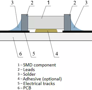
Do not place the vias on the solder pads because soldering in a reflow oven may result in the sucking the paste located on the solder pad into the interior of vias, which may further result in too weak soldering of the component and poor electrical connection between the component lead and the solder pad.
- 8. Bonding components and assembly layer
It is recommended to use only one assembly layer to attach components at the SMT assembly. Sometimes, however, this is impossible. As a result of e.g. high density of the components in a single PCB layer, it is necessary to use two layers - top and bottom.
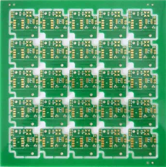
When soldering includes two assembly layers, on one of them in areas in where electronic components are to be attached, in addition to the soldering paste adhesive is used. After the application of the adhesive to the first layer the components are assembled on it, then the PCB goes to a reflow oven. Followed by soldering of a given assembly layer and hardening of the adhesive fixing the components. Then, after the PCB is reversed and the components on the other side are soldered in the reflow oven (adhesive on the second layer may be omitted), although the solder on the first layer melts, the adhesive does not allow any movement or drop-off of large (and heavy) electronic components previously superposed on it. - 9. Panelization (Multiblock)
In the case of very small overall dimensions of PCBs or PCBs of special shapes (which are difficult to attach into the Pick & Place machine) is recommended to use panelization, i.e. grouping of individual PCBs into panels. Then, in the process of applying the paste, automatic assembly and solder in the reflow oven, all PCBs located in the panel are soldered at one time. Upon completion soldering, the panel is separated to the individual PCBs, using a separator.
- 10. Soldermask
It is very important that a PCB contains a soldermask layer as the layer protects against the formation of short circuits between solder points located in close proximity. As reflow oven is used during soldering, "confluence" of solder and the creation of "bridges" on the adjacent solder pads would result from not using the soldermask. Soldermask may not overlap the pad but can be located in very close to it (up to approx. 0.05 mm).
- 11. Steel stencils for solder paste application
Stencils for the application of solder paste (and/or adhesive) are made from precision stainless sheet steel with a thickness of 0.1 to 0.3 mm. According to the recommendations of the Customer or in the case of assembly components whose pitch is greater than or equal to 0.5 mm, stencils are made by etching (much lower price but slightly worse quality). In case of assembly components whose pitch is less than 0.5 mm, the stencils are cut with a laser beam (high price but high quality).
At the Customer’s request we store the stencils (or send to the Customer) in order to accelerate the launch of the production line in the event the same order is placed again.NOTE! When the stencil is provided by the Customer it is required that the stencil has designed perforation applied (with holes of appropriate spacing and diameter suitable for coupling the frame in our stencil printer). In order to facilitate the stencil perforation design the picture below demonstrates the technical drawing of mounting frame (click the thumbnail to display the picture in full size). In addition, we have prepared a 3D model (dimensioned) in * .STEP format.


- 12. Development of the assembly program
We usually develop assembly program using hardware project sent by the Customer and the Pick&Place file generated from this project by means of EDA software.
The hardware may be made in the following design environments:- Payable: Altium Designer/Protel, Cadence OrCad, Zuken CADSTAR, Proteus VSM
- Free: Autotrax, Eagle, KiCAD….
At Customer’s request we store developed program (or send to the Customer) in order to accelerate any subsequent launch of the production line in the event the same contract is resumed.
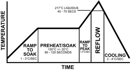
- 13. Soldering profile
The profile of work temperature of reflow oven (soldering profile) is determined based on the documentation of assembled electronic components (to determine their resistance temperature) as well as on the basis of the characteristics of PCB high temperature resistance.
- 1. Reference points (fiducials) and their implementation
- IV. THT assembly (Through-Hole Technology):
- 1. When to apply?
In today's electronics mainly surface mount (SMT) is prevails due to very small size of SMD components (owing to which the dimension of the final device is decreased) and high speed of assembly. Components intended for through-hole assembly (THT) should be used when mechanical forces may be exerted or the casing of the required component used in a given electronic system does not have its SMD equivalent.
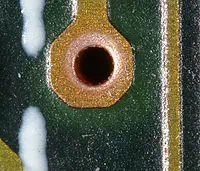
Through-hole technology is most often used to attach slots or ports that are particularly exposed to mechanical damage. Very high mechanical strength is obtained by depositing component leads into mounting holes. SMD components are much less mechanically resistant. Too much force applied may result in the detachment of PCBs, often in conjunction with the soldering points and parts of tracks directly connected to these points.
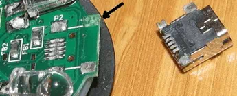
Ripped out USB port (SMT technology)
with solder pad and a piece of track - 2. Our capabilities
For single-sided through-hole assembly (one layer) we use wave soldering unit that allows to automate soldering process. The components are placed on the PCB manually.Double-sided through-hole assembly (Top and Bottom layer) is made on a Customer’s request. It is made using a solder wave unit or manually and is limited to specific cases (including assembly of sockets, connectors, ports, or components exposed to mechanical damages).
- 1. When to apply?
- V. Glossary Terms:
- 1. PCB - Printed circuit board
PCB – Printed Circuit Board – a board made of insulating material with electrical connections (i.e. tracks) and solder points, for electronic components assembly. Printed circuits are designed for electronics and are made as a result of etching process. They are produced from a board covered with a cooper layer where a wiring pattern is placed (most often printed) onto using various technology and then, to obtain a desired pattern, chemical treatment is applied (see: Wikipedia).
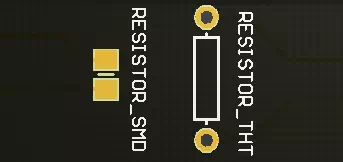
- 2. SMT assembly – Surface Mount Technology SMT – Surface Mount Technology – a method of assembling electronic components on the circuit board where the solder pads are located on the same layer as assembled components. It features a higher condensation of components on a PCB than THT assembly, which allows to miniaturize the assembled device. Owing to low connection impedance, the efficiency of the circuits operating at high frequencies is increased. SMT assembly is much cheaper than THT assembly (see: Wikipedia).
- 3. SMD components
SMD – Surface Mounted Devices – electronic components for surface mounting - components of small size with flat packages and soldering pins in the form of flanges covering the ends of the package. Due to lower weight of components, a finished device demonstrates good mechanical properties during shock or vibration (see: Wikipedia).
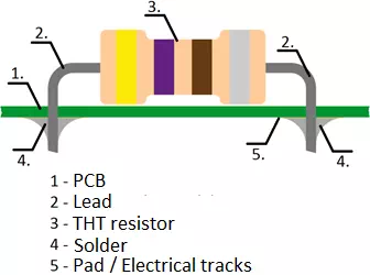
- 4. THT assembly (Through-Hole Technology)
THT – Through-Hole Technology – a method for mounting electronic components on a printed circuit board (PCB). Electronic components for mounting to the hole are equipped with wires which are threaded through holes in the PCB during assembly and soldered to the conducting tracks on the opposite side of the PCB than the mounting component (see: Wikipedia).
- 5. Via
Via – electric transition between layers of PCB (eg. TOP and BOTTOM). It is a metallic plated (copper plated) hole with a small diameter with a ring on each of the merged layers, which connects the track or tracks located on the given layer. In the printed circuit board, selection of appropriate types of vias has a decisive influence on the degree of miniaturization of the whole system and the production price (see: Wikipedia).
- 6. Solder pad Pad – a field which is an electrical contact of a PCB track / tracks with electrode (pin/lead) of electronic component that performs the function of fastening the electronic component to a PCB via solder, being the conductor at the same time. Solder pads are used in SMT and THT (in the case of THT – as a hole with a ring).
- 7. Soldermask Solder mask – varnish (usually green but other colors are also used) or a polymer which is applied directly to the copper on the printed circuit board without copper parts such as solder pads or vias (not always). Soldermask protects the copper against mechanical damage, oxidation and "confluence" (causing a short circuit) of solder from two solder points. In addition, solder mask also protects to some degree against electric shocks as it is a good insulator (see: Wikipedia).
- 8. Fiducial Fiducial – a small marker that allows automatic assembly machine (if equipped with a vision system) to determine the position of a PCB and apply corrections so that the components are always located precisely. If PCBs are components of a small pin pitch and a large number of feet (e.g. BGA) it is worth also to use local fiducials that include a single electronic component (see: Wikipedia).
- 9. SMT stencil SMT Stencil – most usually made of sheet metal (0.1 - 0.3 mm) stainless steel stencil, is used for precise application of solder paste on solder pads (solder paste going through holes in the stencil). It is most frequently made by etching or laser-cut techniques (high quality) - see: Wikipedia.
- 10. Panelization/Depanelization
Panelization/Depanelization – a solution to facilitate the implementation of a series of PCBs, where after the design of a single PCB, it is automatically duplicated (in the program for the design of printed circuit boards) in order to place on one large-size PCB panel. Circuit boards are supplied on large sheets (panels) and then into single copies by means of a separator. In general, the orientation of PCB on a panel is arranged by the manufacturer. In the case of change of PCB contractor, make sure that the PCB in the sheet are arranged in the same way with identical distance from each other (see: Wikipedia).
- 11. Thermal profile / Soldering profile Thermal profiling – a precise temperature distribution used in various phases of work in a reflow oven. It involves the measurement of temperature at several points on a PCB intended for a reflow oven and the adjustment of heating temperature in a given time interval. This is very important since too rapid heating of the solder paste may result in "splashing" (and thus - very poor quality solder connections) or "the dissolution" leading to short circuits between the solder pads located close to each other, or even "popcorn" effect (bursting of the component package). Thermal profile defines the temperature distribution in the following phases of operation of the reflow oven:
- preheat;
- soak;
- reflow;
- cooling.
Temperature range set on a reflow oven is highly dependent on the type and chemical composition of the solder paste applied as well as on heat resistance of mounted components and PCB (see: Wikipedia).
- 12. Reflow soldering
Reflow soldering – soldering technique of electronic components (SMD) by the means of a reflow oven, which consists of several stages:
- application of solder paste on solder pads by using SMT stencil;
- mounting of SMD components using SMT machine;
- placement of PCB in a reflow oven (programmed soldering profile) featuring several heating zones.
To heat PCB circuits in reflow ovens, most often in use are infra-red heaters or forced convection of hot air or an inert gas, e.g.: Nitrogen (see: Wikipedia).
- 13. Wave soldering
Wave soldering – soldering technique of electronic components (THT) using the unit for wave soldering. This technique involves several stages:
- Fluxing, involving solder flux on the PCB side;
- Heating, in order to dry and activate the flux and to preheat the PCB in order to avoid thermal shock (leading to distortion of the PCB and internal stress);
- Soldering, meaning moving the PCB by means of a conveyor to the crest of a wave of molten solder. The lower part of the PCB (soldered) is in contact with the back wave, wherein the solder is fixed to form a permanent solder connection. This process takes from 3 to 10 seconds (see: Wikipedia).
- 1. PCB - Printed circuit board
Electronics manufacturing services (SMT assembly and THT assembly) - Knowledge base
- Also available:
")
")
")